- 您现在的位置:买卖IC网 > Sheet目录471 > MAX2032ETP+ (Maxim Integrated)IC MIXER UP/DOWN CONVER 20TQFN
High-Linearity, 650MHz to 1000MHz Upconversion/
Downconversion Mixer with LO Buffer/Switch
ABSOLUTE MAXIMUM RATINGS
V CC to GND ...........................................................-0.3V to +5.5V
RF (RF is DC shorted to GND through a balun)..................50mA
LO1, LO2 to GND ..................................................-0.3V to +0.3V
IF+, IF- to GND ...........................................-0.3V to (V CC + 0.3V)
TAP to GND ...........................................................-0.3V to +1.4V
LOSEL to GND ...........................................-0.3V to (V CC + 0.3V)
LOBIAS to GND..........................................-0.3V to (V CC + 0.3V)
Continuous Power Dissipation (Note 2)....................................5W
θ JA (Notes 3, 4)..............................................................+38°C/W
θ JC (Notes 2, 3)..............................................................+13°C/W
Operating Temperature Range (Note 5) .....T C = -40°C to +85°C
Junction Temperature ......................................................+150°C
Storage Temperature Range .............................-65°C to +150°C
Lead Temperature (soldering, 10s) .................................+300°C
RF, LO1, LO2 Input Power (Note 1) ...............................+20dBm
Note 1: Maximum, reliable, continuous input power applied to the RF and IF port of this device is +12dBm from a 50 ? source.
Note 2: Based on junction temperature T J = T C + ( θ JC x V CC x I CC ). This formula can be used when the temperature of the exposed
pad is known while the device is soldered down to a PCB. See the Applications Information section for details. The junction
temperature must not exceed +150°C.
Note 3: Package thermal resistances were obtained using the method described in JEDEC specification JESD51-7, using a four-
layer board. For detailed information on package thermal considerations, refer to www.maxim-ic.com/thermal-tutorial .
Note 4: Junction temperature T J = T A + ( θ JA x V CC x I CC ). This formula can be used when the ambient temperature of the PCB is
known. The junction temperature must not exceed +150°C.
Note 5: T C is the temperature on the exposed pad of the package. T A is the ambient temperature of the device and PCB.
Stresses beyond those listed under “Absolute Maximum Ratings” may cause permanent damage to the device. These are stress ratings only, and functional
operation of the device at these or any other conditions beyond those indicated in the operational sections of the specifications is not implied. Exposure to
absolute maximum rating conditions for extended periods may affect device reliability.
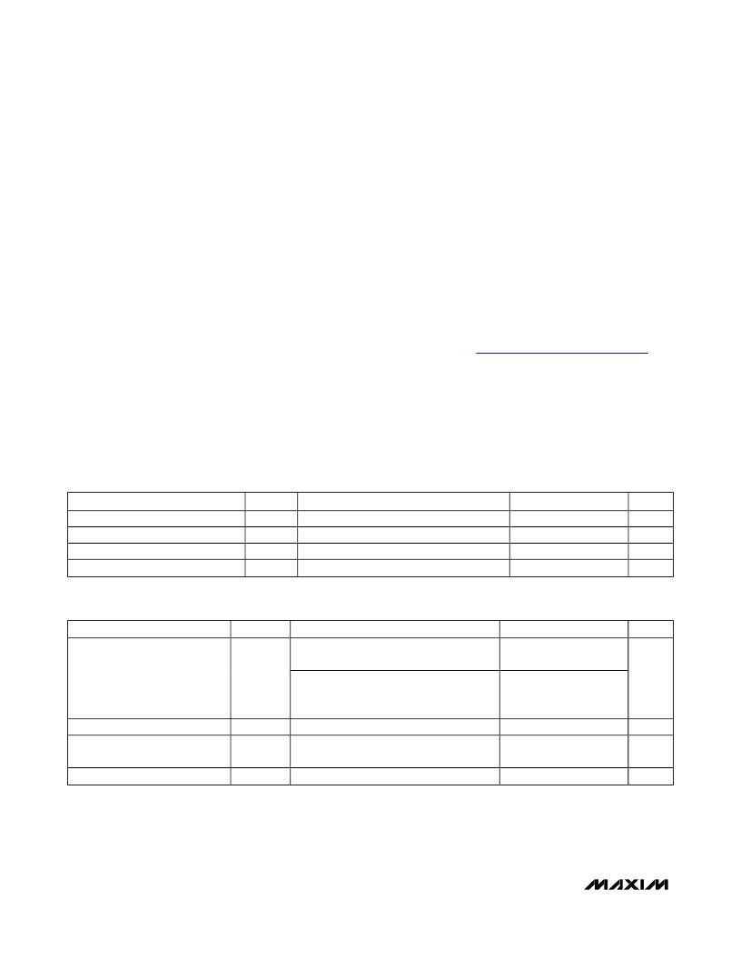
DC ELECTRICAL CHARACTERISTICS
(Typical Application Circuit, V CC = 4.75V to 5.25V, no RF signals applied, T C = -40°C to +85°C. IF+ and IF- are DC grounded through an
IF balun. Typical values are at V CC = 5V, T C = +25°C, unless otherwise noted.)
PARAMETER
Supply Voltage
Supply Current
SYMBOL
V CC
I CC
CONDITIONS
MIN
4.75
TYP
5.00
85
MAX
5.25
100
UNITS
V
mA
LOSEL Input Logic-Low
LOSEL Input Logic-High
V IL
V IH
2
0.8
V
V
RECOMMENDED AC OPERATING CONDITIONS
PARAMETER
SYMBOL
CONDITIONS
MIN
TYP
MAX
UNITS
Components tuned for the 700MHz band
(Table 1), C1 = 7pF, C5 = 3.3pF (Notes 6, 7)
650
850
RF Frequency
f RF
Components tuned for the 800MHz/900MHz
cellular band (Table 1), C1 = 82pF,
800
1000
MHz
C5 = 2.0pF (Note 6)
LO Frequency
IF Frequency
LO Drive Level
f LO
f IF
P LO
(Notes 6, 7)
IF frequency range depends on external IF
transformer selection
(Note 6)
650
0
-3
1250
250
+3
MHz
MHz
dBm
2
_______________________________________________________________________________________
发布紧急采购,3分钟左右您将得到回复。
相关PDF资料
MAX2034CTM+
IC AMP LOW NOISE QUAD 48-TQFN
MAX2035EVKIT
EVAL KIT FOR MAX2035
MAX2039ETP+D
IC MIXER UP/DWN HI LIN 20-TQFN
MAX2039EVKIT
EVAL KIT FOR MAX2039
MAX2041ETP+T
IC MIXER UP/DWN HI LIN 20-TQFN
MAX2041EVKIT
EVAL KIT FOR MAX2041
MAX2042AETP+T
IC UP/DWN CONVERSION MIXR 20TQFN
MAX2042ETP+T
IC MIXER UP/DOWN CONVER 20TQFN
相关代理商/技术参数
MAX2032ETP+T
功能描述:射频混合器 .65GHz-1GHz Up/Down Mixer RoHS:否 制造商:NXP Semiconductors 频率范围: 转换损失——最大: 工作电源电压:6 V 最大工作温度:+ 85 C 最小工作温度:- 40 C 安装风格:Through Hole 封装 / 箱体:PDIP-8 封装:Tube
MAX2034
制造商:MAXIM 制造商全称:Maxim Integrated Products 功能描述:Quad-Channel, Ultra-Low-Noise Amplifier with Digitally Programmable Input Impedance
MAX2034CTM
功能描述:射频放大器 RoHS:否 制造商:Skyworks Solutions, Inc. 类型:Low Noise Amplifier 工作频率:2.3 GHz to 2.8 GHz P1dB:18.5 dBm 输出截获点:37.5 dBm 功率增益类型:32 dB 噪声系数:0.85 dB 工作电源电压:5 V 电源电流:125 mA 测试频率:2.6 GHz 最大工作温度:+ 85 C 安装风格:SMD/SMT 封装 / 箱体:QFN-16 封装:Reel
MAX2034CTM+
功能描述:射频放大器 4Ch Amp w/Digital Prog Input Imp RoHS:否 制造商:Skyworks Solutions, Inc. 类型:Low Noise Amplifier 工作频率:2.3 GHz to 2.8 GHz P1dB:18.5 dBm 输出截获点:37.5 dBm 功率增益类型:32 dB 噪声系数:0.85 dB 工作电源电压:5 V 电源电流:125 mA 测试频率:2.6 GHz 最大工作温度:+ 85 C 安装风格:SMD/SMT 封装 / 箱体:QFN-16 封装:Reel
MAX2034CTM+T
功能描述:射频放大器 4Ch Amp w/Digital Prog Input Imp RoHS:否 制造商:Skyworks Solutions, Inc. 类型:Low Noise Amplifier 工作频率:2.3 GHz to 2.8 GHz P1dB:18.5 dBm 输出截获点:37.5 dBm 功率增益类型:32 dB 噪声系数:0.85 dB 工作电源电压:5 V 电源电流:125 mA 测试频率:2.6 GHz 最大工作温度:+ 85 C 安装风格:SMD/SMT 封装 / 箱体:QFN-16 封装:Reel
MAX2034CTM-T
功能描述:射频放大器 RoHS:否 制造商:Skyworks Solutions, Inc. 类型:Low Noise Amplifier 工作频率:2.3 GHz to 2.8 GHz P1dB:18.5 dBm 输出截获点:37.5 dBm 功率增益类型:32 dB 噪声系数:0.85 dB 工作电源电压:5 V 电源电流:125 mA 测试频率:2.6 GHz 最大工作温度:+ 85 C 安装风格:SMD/SMT 封装 / 箱体:QFN-16 封装:Reel
MAX2035
制造商:MAXIM 制造商全称:Maxim Integrated Products 功能描述:Ultrasound Variable-Gain Amplifier
MAX2035_09
制造商:MAXIM 制造商全称:Maxim Integrated Products 功能描述:Ultrasound Variable-Gain Amplifier
